


アルミニウム PCB、銅コア PCB、セラミック PCB およびメタル コア PCB ガイド
熱管理が PCB 基板の選択を決定する理由
標準 FR-4 ガラスエポキシ プリント基板は、ほとんどの汎用電子機器の熱要求に適切に対応します。しかし、パワー エレクトロニクス、高輝度 LED システム、RF およびマイクロ波モジュール、自動車制御ユニット、産業用モーター ドライブでは、単位面積あたりに発生する熱が FR-4 が能動部品から伝導できる熱を超え、接合部温度の上昇、エレクトロマイグレーションの加速、部品寿命の短縮、そして最終的には熱故障につながります。基板自体の熱性能が設計上の拘束条件となる場合、エンジニアは特殊なボードのファミリーに注目します。 メタルコアPCB 、 アルミニウム基板 、 銅コアPCB 、 and セラミックPCB .
これらの基板技術はそれぞれ、異なる物理メカニズムを通じて FR-4 の熱制限に対処しており、それぞれが熱伝導率、電気絶縁、機械的特性、コスト、製造容易性において明確なトレードオフをもたらします。適切な基板を選択するには、各タイプが単独で何を提供するかだけでなく、それらの特性が特定の電力密度、動作環境、フォームファクター、およびアプリケーションの信頼性目標とどのように相互作用するかを理解する必要があります。
メタルコア基板 : 広範なカテゴリとその定義構造
あ メタルコアPCB (MCPCB) は、従来の FR-4 またはその他のポリマー複合コアの代わりに金属プレートを使用するプリント基板の総称です。金属コアは統合されたヒート スプレッダーとして機能し、表面実装コンポーネントによって生成された熱をその高伝導面全体で横方向に引き出し、それを取り付けられたヒートシンクまたはシャーシに下方に伝達し、従来の PCB 構造で熱の流れを妨げる熱抵抗ポリマー層をバイパスします。
標準のメタル コア PCB スタックアップは、次の 3 つの機能層で構成されます。
- 金属ベース層: 構造コアと熱コア (アルミニウム、銅、場合によってはスチール) は通常、厚さが 0.8 ~ 3.0 mm で、機械的剛性と主な熱伝導経路を提供します。
- 誘電体絶縁層: あ thermally conductive but electrically insulating polymer film — typically filled epoxy, polyimide, or ceramic-loaded resin — bonded between the metal base and the copper circuit layer. This layer is the thermal bottleneck of the stack and its thermal conductivity (measured in W/m·K) is the most critical specification in MCPCB selection. Standard dielectric layers achieve 1–3 W/m·K; advanced ceramic-filled dielectrics reach 6–10 W/m·K.
- 銅回路層: あ patterned copper foil (typically 1–4 oz/ft²) carrying the electrical interconnect, etched by standard PCB photolithography processes.
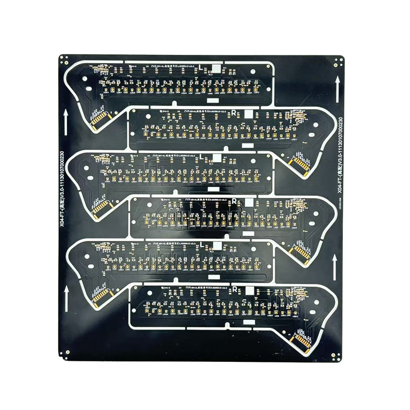
メタル コア PCB は、ほとんどの場合片面です (一方の面には回路層、もう一方の面にはベアメタル ベース)。これは、ある銅層から別の銅層へのスルーホール ビアがメタル コアに直接短絡するためです。両面および多層の MCPCB 構造は存在しますが、特殊な絶縁ビア技術が必要であり、コストが大幅に増加します。 LED ドライバー、電源モジュール、モーター コントローラーのアプリケーションの大部分では、片面 MCPCB で十分かつ最適です。
あluminum PCB : コスト効率の高い熱管理の業界標準
の アルミニウム基板 — メタル コア PCB の最も広く製造されている変種 — は、熱的および構造的コアとしてアルミニウム合金ベース プレート (最も一般的には 5052 または 6061 シリーズ) を使用します。アルミニウムは、適度な熱伝導率 (一般的な合金で約 160 ~ 205 W/m·K)、低密度、良好な機械加工性、低コストの組み合わせにより、FR-4 では不十分だが用途が銅やセラミック基板のプレミアムを正当化できない場合のデフォルトの選択肢となります。
の real-world thermal performance of an aluminum PCB is determined primarily by the dielectric layer, not the aluminum base itself. A standard 75 µm dielectric at 1 W/m·K creates a thermal resistance of approximately 7.5 °C·cm²/W between the component mounting surface and the aluminum base — a value that dominates the total thermal budget and significantly limits the effective advantage of the metal core over a high-quality thermal interface material on an FR-4 board with an external heatsink. Upgrading to a 100 µm ceramic-filled dielectric at 6 W/m·K reduces this interface resistance to approximately 1.7 °C·cm²/W, yielding a dramatically lower component junction temperature for the same power dissipation.
あluminum PCBs dominate the following application segments:
- LED照明: 街路照明、産業用高天井、園芸、自動車ヘッドランプ用途向けの高輝度 LED アレイは、アルミニウム PCB の単一市場としては最大です。このボードは、LED キャリア、回路相互接続、および照明器具ハウジングへの主要なヒート スプレッダとして同時に機能します。
- 電源とコンバータ: MOSFET、ダイオード、およびインダクタを搭載したスイッチモード電源ボードは、別個のヒートシンク アセンブリを必要とせずに、コンポーネントのケースから周囲までの熱抵抗を低減するアルミニウム ベースの恩恵を受けます。
- あutomotive electronics: 電気自動車およびハイブリッド自動車の ECU パワー ステージ、LED ドライバー モジュール、およびバッテリー管理システム ボードでは、熱性能、耐振動性、および標準 SMT アセンブリ プロセスとの互換性を組み合わせるために、アルミニウム PCB が使用されています。
- モータードライブとインバーター: 可変周波数ドライブとサーボ アンプは、ドライブ シャーシまたはヒートシンクの押し出し部分に直接ボルトで固定されるアルミニウム PCB にゲート ドライバー回路とパワー デバイスを取り付けます。
銅コアPCB : メタルコア構造の最大熱伝導率
あ 銅コアPCB アルミニウムのベース プレートを銅または銅合金のコアに置き換え、金属層の熱伝導率を約 160 ~ 200 W/m·K (アルミニウム) から約 200 W/m·K に高めます。 385~400W/m・K — アルミニウムの約 2 倍の熱伝導率。この違いは、熱勾配によってジャンクション温度がコンポーネントの定格制限を超える前に、小さなソース領域から熱を急速に拡散させる必要がある、局所的な電力密度が極端に高いアプリケーションで最も顕著です。
の performance advantage of copper core over aluminum core is most pronounced when:
- 電力密度は、局所的なコンポーネントの設置面積で約 15 ~ 20 W/cm2 を超えます。この場合、アルミニウムの横方向の伝導率が低いため、熱が基板の端に広がる前にホット スポットが形成されます。
- の board-to-heatsink interface area is limited by packaging constraints, making lateral heat spreading within the board itself the primary means of distributing load across the interface.
- 熱膨張係数 (CTE) のマッチングは重要です。銅の CTE (~17 ppm/°C) は、アルミニウムの CTE (~23 ppm/°C) よりも一般的な半導体パッケージの CTE に近いため、繰り返しの熱サイクル下ではんだ接合部の熱機械的ストレスが軽減されます。
の primary trade-offs of copper core PCBs are cost and weight. Copper is approximately three times the material cost of aluminum per unit weight, and at 8.9 g/cm³ (versus 2.7 g/cm³ for aluminum), a copper core board of the same dimensions is roughly 3.3 times heavier. These factors restrict copper core PCBs to applications where thermal performance genuinely justifies the premium — high-power laser diode drivers, IGBT gate driver boards, radar transmitter modules, and precision power amplifiers are representative examples.
あn important variant is the 埋め込み銅コイン PCB 、 in which a copper slug is press-fitted or plated into a localized region of an otherwise standard FR-4 or aluminum PCB directly beneath a high-power component. This approach delivers copper-level thermal performance precisely where it is needed, without converting the entire board to a copper core — significantly reducing cost and weight relative to a full copper core construction.
セラミック基板 : 極限環境向けのプレミアムチョイス
あ セラミック基板 メタルコア構造から完全に離れ、代わりにモノリシックセラミック基板(最も一般的には酸化アルミニウム(Al₂O₃)、窒化アルミニウム(AlN)、または窒化ケイ素(Si₃N₄))を機械的ベースと熱伝導性誘電体の両方として使用します。セラミックは本質的に電気絶縁性であるため、基板と銅回路層の間に別の誘電体膜は必要ありません。これにより、MCPCB の性能を制限する熱抵抗ポリマーの界面が排除され、セラミック表面のミクロン以内にコンポーネントを実装できるようになります。
の three principal ceramic substrate materials span a wide range of thermal performance and cost:
- あluminum oxide (Al₂O₃, 96% and 99.6% purity): のrmal conductivity of 24–35 W/m·K. The most cost-effective ceramic substrate, widely used in thick-film hybrid circuits, sensor modules, and RF substrates. Mechanically strong and chemically inert, but its thermal conductivity is substantially lower than AlN — adequate for moderate power densities but insufficient for high-power applications where temperature rise must be minimized.
- あluminum nitride (AlN): のrmal conductivity of 140–180 W/m·K — approaching that of aluminum metal — combined with a CTE of approximately 4.5 ppm/°C that closely matches silicon (2.6 ppm/°C) and GaAs (5.7 ppm/°C). AlN ceramic PCBs are the substrate of choice for power semiconductor modules, high-brightness LED flip-chip arrays, RF power amplifiers, and aerospace electronics operating at elevated temperatures. The CTE match to silicon virtually eliminates thermo-mechanical fatigue at die attach interfaces under thermal cycling, enabling long-term reliability in mission-critical applications.
- 窒化ケイ素 (Si₃N₄): のrmal conductivity of 60–90 W/m·K combined with exceptional mechanical toughness (fracture toughness ~7 MPa·m½, versus ~3–4 MPa·m½ for AlN). Silicon nitride ceramic PCBs are specified where both high thermal conductivity and resistance to mechanical shock, vibration, and thermal shock are required simultaneously — electric vehicle power modules, railway traction inverters, and wind turbine converter boards are primary applications.
銅回路は、次の 2 つの主要なプロセスによってセラミック基板に接着されます。 ダイレクトボンド銅 (DBC) 、 in which a copper foil is bonded to the ceramic surface by a controlled eutectic reaction at approximately 1065 °C, and 活性金属ろう付け(AMB) 、 which uses a silver-copper-titanium braze alloy to bond copper to the ceramic at lower temperature with superior bond strength. DBC on AlN is the dominant technology for power module substrates; AMB is preferred for silicon nitride substrates and for applications requiring the highest thermal cycling reliability.
4 種類すべての基板の性能比較
| パラメータ | あluminum PCB | 銅コアPCB | あl₂O₃ Ceramic PCB | あlN Ceramic PCB |
|---|---|---|---|---|
| コアの熱伝導率 | 160~205W/m・K | 385~400W/m・K | 24~35W/m・K | 140~180W/m・K |
| 誘電体層は必要ですか? | はい | はい | いいえ | いいえ |
| CTE (ppm/℃) | ~23 | ~17 | ~7 | ~4.5 |
| 最高使用温度 | ~140 °C (誘電制限) | ~140 °C (誘電制限) | >350 °C | >350 °C |
| 相対的な材料コスト | 低い | 中~高 | 中 | 高 |
| 被削性 | 素晴らしい | 良い | 難しい(脆い) | 難しい(脆い) |
| 一般的な最小フィーチャ サイズ | 100μm | 100μm | 75~100μm | 75~100μm |
あpplication Mapping: Choosing the Right Substrate for Your Design
の decision tree for substrate selection starts with power density and operating temperature, then factors in mechanical environment, reliability target, and cost budget:
- 電力密度 10 W/cm² 未満、動作温度 105 °C 未満、コスト重視の量産: 1 ~ 3 W/m·K の誘電体を備えた標準アルミニウム PCB が、適切かつ最も経済的な選択です。 LED 照明、民生用電源、汎用モーター コントローラーなどがこのカテゴリに分類されます。
- 電力密度 10 ~ 25 W/cm²、熱サイクル要件、中程度のコスト許容度: あluminum PCB with a high-performance 6–10 W/m·K ceramic-filled dielectric, or a copper core PCB where lateral spreading is the primary need. Automotive LED modules, DC-DC converter power stages, and industrial servo drives are representative.
- 電力密度 25 W/cm² 以上、ベアダイ アセンブリ、動作温度 150 °C 以上: あlN ceramic PCB (DBC or AMB) is required. Power semiconductor modules for EV traction inverters, SiC and GaN device substrates, and high-power RF amplifiers for base stations and radar all demand AlN ceramic performance.
- 高い機械的衝撃と振動と高い出力密度の組み合わせ: 窒化ケイ素セラミック PCB は、鉄道牽引、航空宇宙、および重工業用インバータ用途に必要な、高い熱伝導率と破壊靱性の独自の組み合わせを実現します。
- 制御された誘電率と低損失正接を必要とする RF およびマイクロ波回路: あl₂O₃ ceramic PCB provides the stable, low-loss dielectric environment required for microwave hybrid circuits, phased array antenna elements, and precision oscillator substrates where polymer-based boards exhibit unacceptable dielectric variation with temperature and humidity.
製造および設計に関する考慮事項
各基板タイプには、基板の選択を決定する前に理解する必要がある特定の設計ルールと製造上の制約が課せられます。
- あluminum and copper core PCBs FR-4 ボードと同様に、はんだペーストの印刷、ピック アンド プレース、およびリフローはんだ付けが行われ、若干の変更を加えた標準 SMT 組立ラインで処理されます。金属ベースには、標準的な PCB ドリルビットではなく超硬工具を使用して穴あけする必要があり、ボードは切り込みを入れたり壊したりするのではなく、配線またはパンチする必要があります。エッジコネクタ領域と取り付け穴の周囲は、金属コアからの電気的絶縁を維持するために慎重な設計が必要です。
- セラミック基板s 本質的に脆いため、標準的な PCB ツールで穴を開けたり、打ち抜いたり、配線したりすると破損することはありません。穴と基板の外形は、焼結前にレーザー切断またはダイヤモンド先端工具で機械加工するか、銅接合後に超高速レーザー (ピコ秒またはフェムト秒) で切断する必要があります。この制約により、セラミック PCB パネルの利用が制限され、MCPCB に比べてピースあたりのコストが大幅に増加します。取り扱いと組み立てには、点荷重とエッジ衝撃を回避する治具が必要です。
- のrmal simulation 素材の選択を最終的に行う前に、これを強くお勧めします。誘電体層の熱抵抗 (MCPCB の場合) またはセラミック基板の導電率 (セラミック PCB の場合) を正確に表す CFD または有限要素熱モデルを使用すると、設計者は、プロトタイプ ツールを作成する前に、選択した基板が最大電力損失ですべてのコンポーネントの接合温度を定格制限内に維持していることを検証できます。
- 表面仕上げの選択 はんだ付け性とワイヤボンドの互換性の両方に影響します。 HASL、ENIG、および OSP 仕上げは、アルミニウムおよび銅コアの PCB で利用できます。ベアダイアセンブリ用の DBC AlN 基板は通常、銅回路層上にニッケル - 金仕上げが施されて供給され、共晶はんだダイアタッチと金またはアルミニウムのワイヤボンディングの両方に対応します。
設計にコストの最適化が必要かどうか アルミニウム基板 、 a high-spreading-performance 銅コアPCB 、 or the extreme thermal and environmental capability of an あlN ceramic PCB 、 the common thread across all メタルコアPCB そしてセラミック基板技術は体系的なエンジニアリングアプローチです。最初に熱要件を定量化し、次に、製品ライフサイクル全体にわたってその要件に最も適した性能、加工性、コストプロファイルを備えた基板を選択します。


 一緒に未来を作りましょう

いつでもお問い合わせください
著作権 © Anhui Hongxin Electronic Technology Co., Ltd. All Rights
予約済み。
privacy
卸売プリント基板サプライヤー、メーカー
![]()
